
POE MANUFACTURING
YOUR GLOBAL TECHNOLOGY
PARTNER
Your trusted global electronics manufacturing partner
20+ years of expertise in electronics manufacturing. From prototypes to mass production, we deliver precision solutions for medical, 5G, robotics, IoT, and power supply applications.
Complete manufacturing from PCB fabrication to final assembly
24H quote, 1-day SMT assembly, 7-day parts sourcing
ISO certified with advanced AOI and X-ray inspection
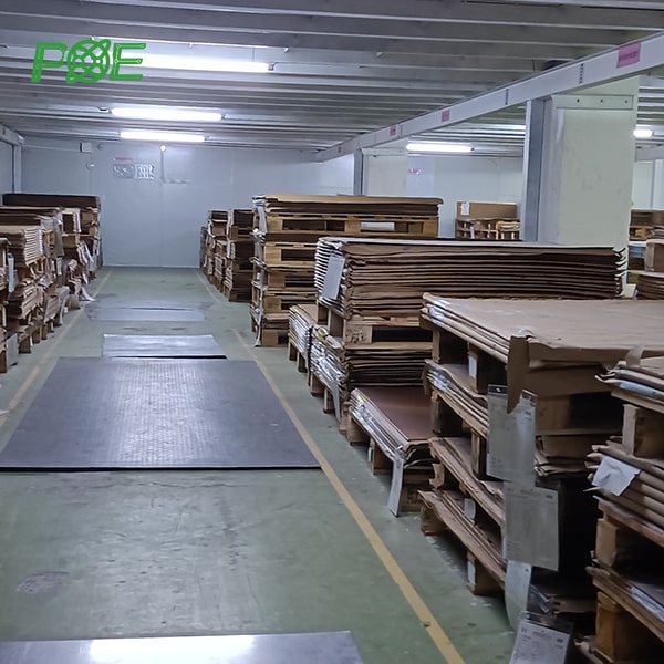
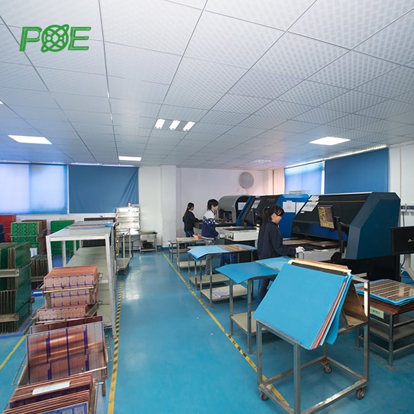
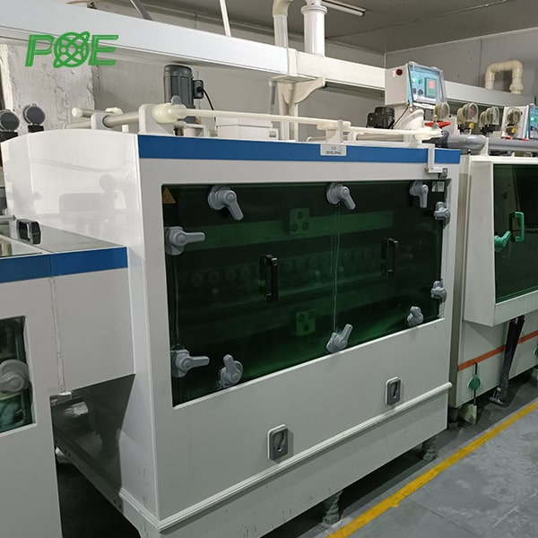
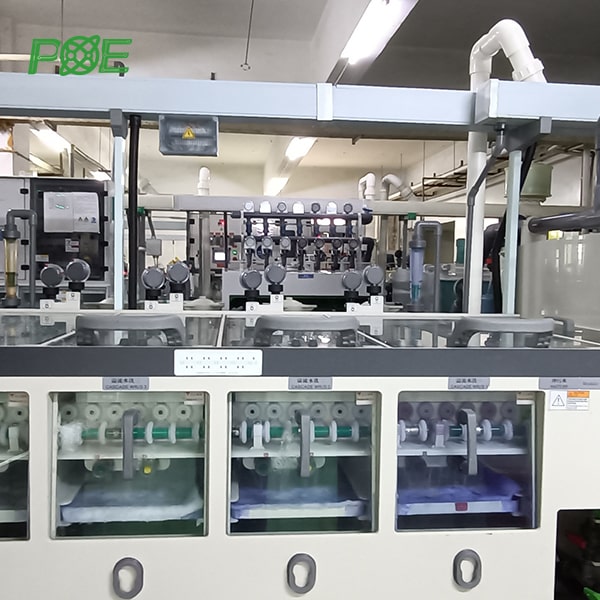
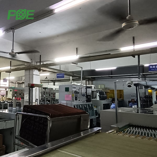
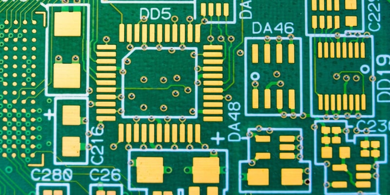
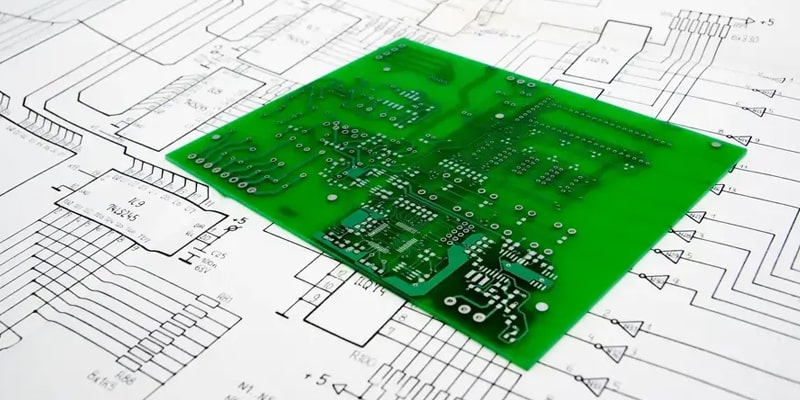
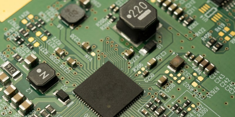
Since 1996, POE has established itself as a leading PCB manufacturer specializing in high-precision printed circuit board fabrication. Our state-of-the-art facility features advanced PCB production lines including multilayer lamination, HDI technology, and rigid-flex capabilities. With dedicated engineering teams across Shenzhen, Hong Kong, and the United States, we deliver superior quality PCB solutions from prototype to mass production. Our PCB manufacturing serves diverse industries including medical devices, 5G telecommunications, automotive electronics, industrial controls, and consumer electronics worldwide.
Premium FR4 substrate preparation and cutting
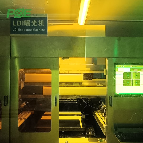
UV lithography for inner layer patterning
Photoresist application and exposure process
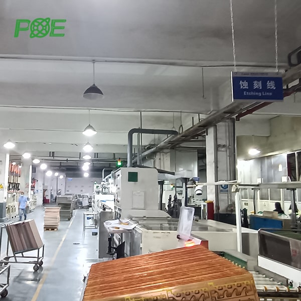
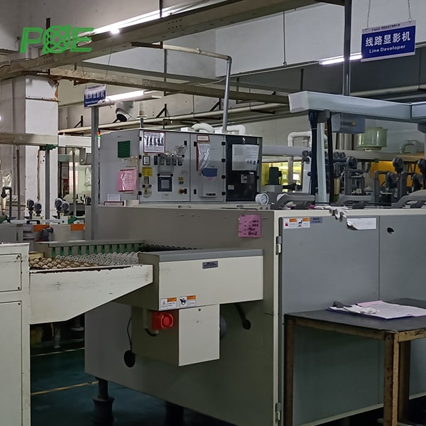
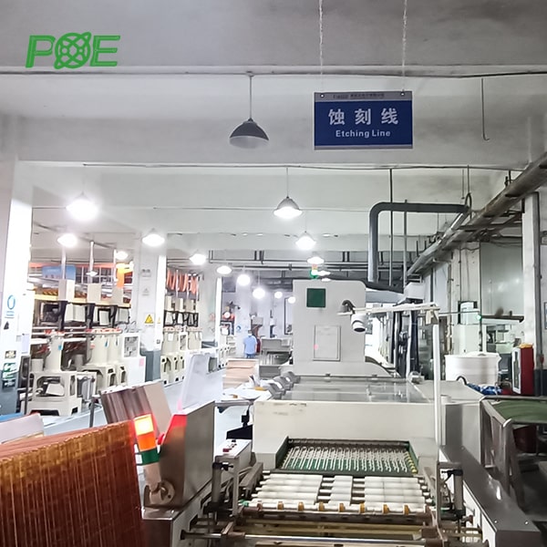
Chemical removal of unwanted copper traces
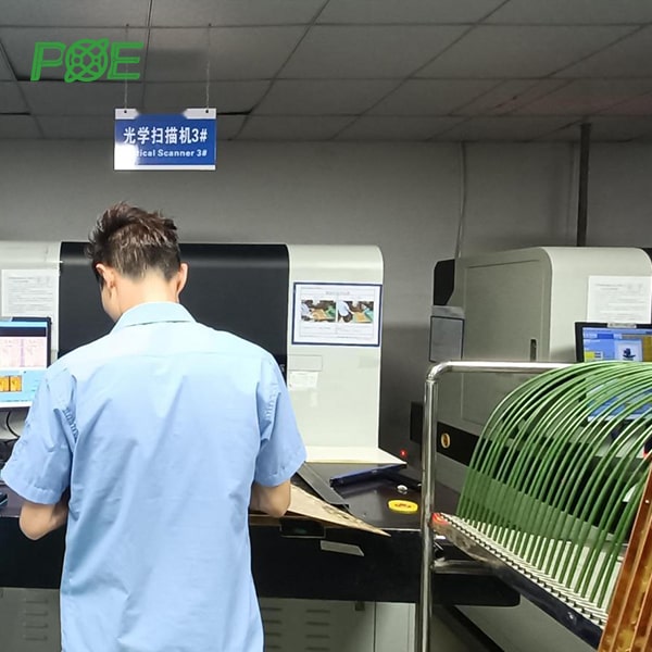
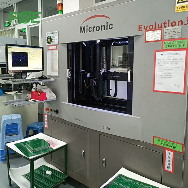
Automated optical verification of inner circuits
Oxide treatment for layer adhesion
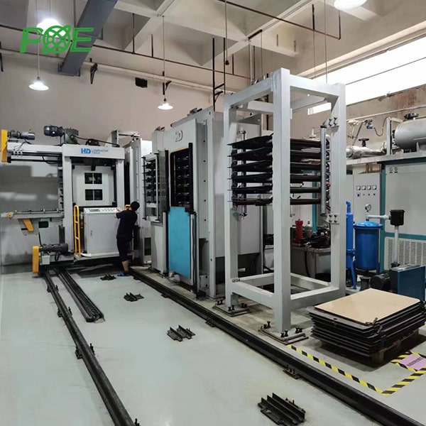
Multi-layer PCB pressing and bonding

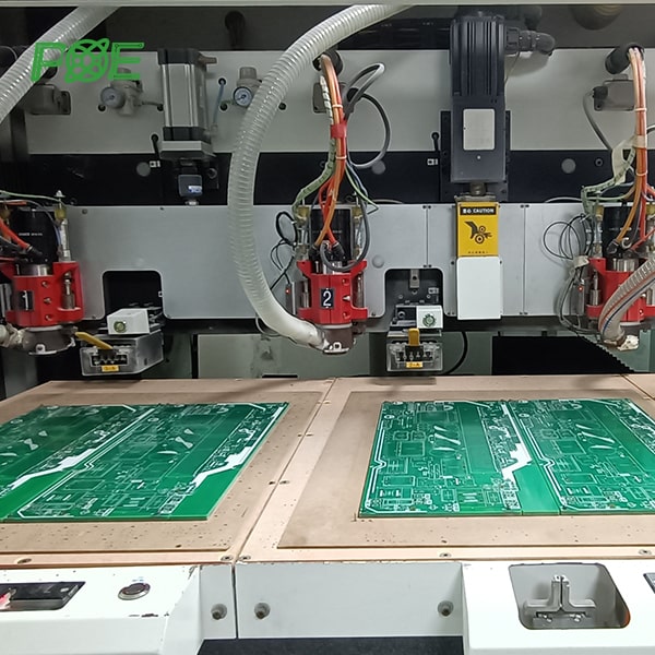
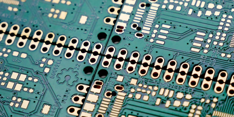
High-precision via and mounting hole drilling
Photoresist removal after processing
Plated through-hole copper deposition
External layer photoresist patterning
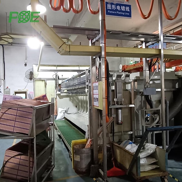
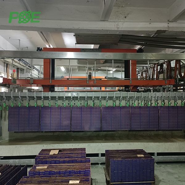
Electroplating copper in drilled holes
Final copper trace definition and cleaning
Final circuit pattern verification
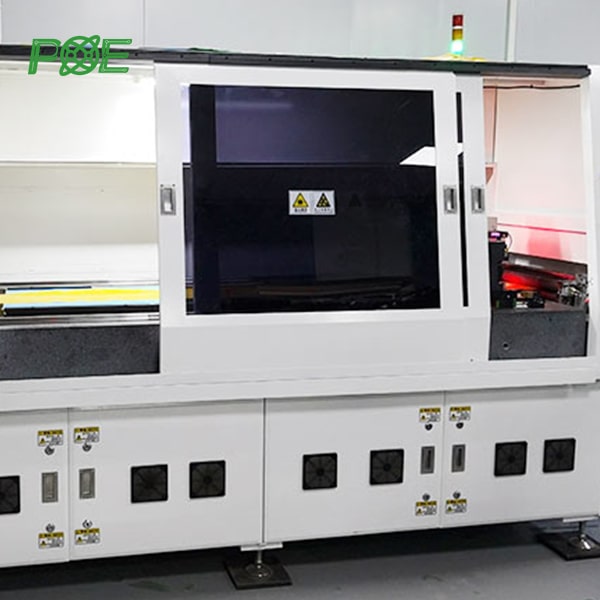
X-ray inspection of internal connections
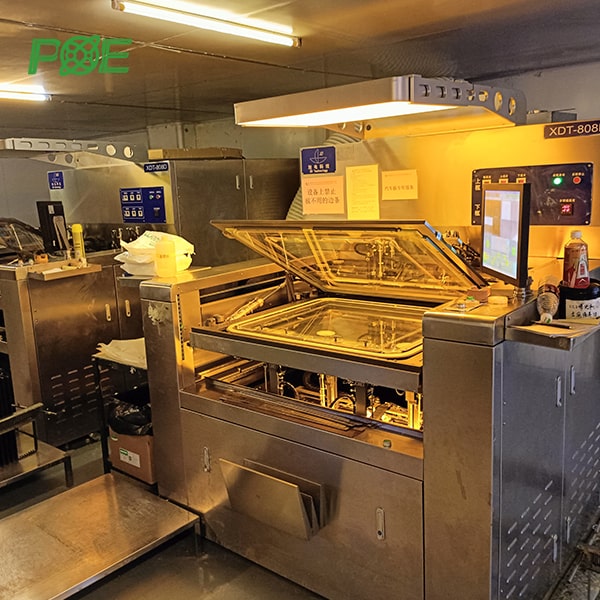
Protective coating application and curing
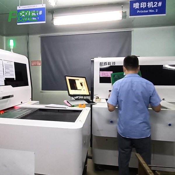
Component legends and marking printing
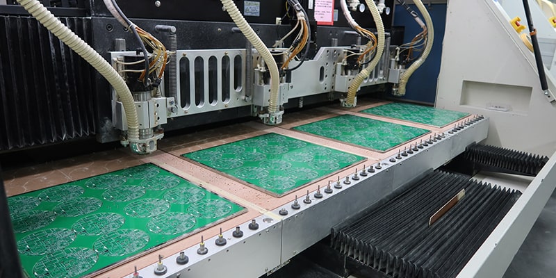
Precision board profiling and routing
Electrical continuity and isolation testing
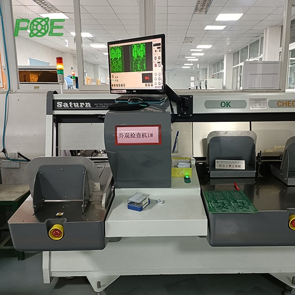
Final quality control and inspection
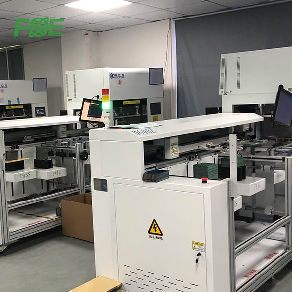
Automated electrical testing system
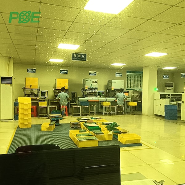
Comprehensive electrical verification
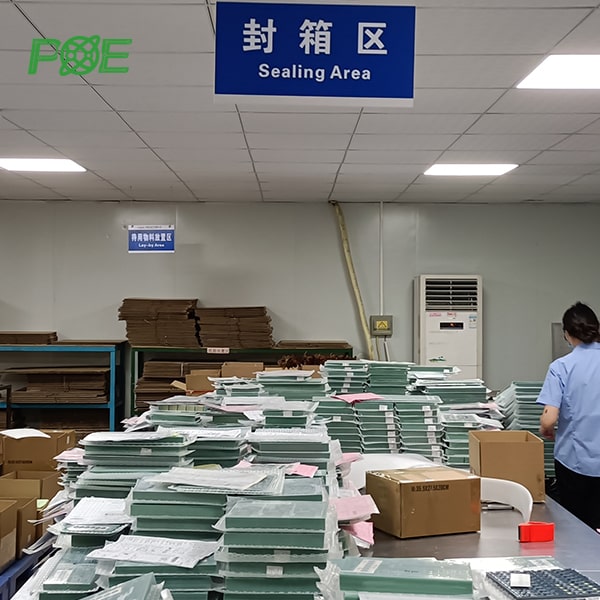
Moisture-free protective packaging

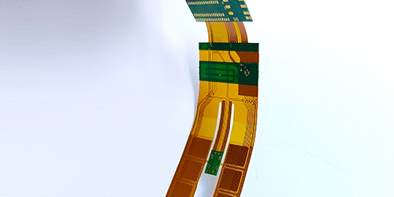

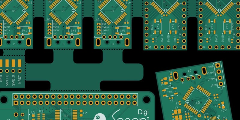
High Density Interconnect PCB manufacturing

4-32 layer PCB fabrication services
HASL, ENIG, OSP, and immersion silver finishes

Electrical testing, AOI, and X-ray inspection
DFM analysis and PCB layout optimization

high-speed
Advanced via-in-pad and via filling technology
Complex via structures
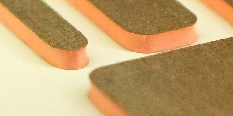
Heavy copper PCB

FR4, Rogers, Polyimide, and specialty substrates
cost-effective production
Complete OEM facility with comprehensive contract manufacturing solutions
35 BOM sourcing engineers offering 1-day quote service
ISO9001:2015 and ISO13485:2016 certified manufacturing
Medical, 5G, Robot, IOT, and Power Supply PCBA solutions


Factory Address:
Floor 3, Jinyuan Industrial Park, No. 56, Tangtou Avenue, Shiyan Town, Baoan District, Shenzhen China

Since 1996, POE has become a globally renowned PCB company, providing small to medium volume PCB/ PCBA manufacturing services.