Web Analytics Made Easy - Statcounter
Multilayer PCB Manufacturing | POE
This website uses cookies:
Our website use cookies to analyze website accesses and improve your online experience. By continuing browsing this website,you agree to our use of cookies and privacy policy.
Accept all cookies
Decline
This website uses cookies:
Our website use cookies to analyze website accesses and improve your online experience. By continuing browsing this website,you agree to our use of cookies and privacy policy.
Accept all cookies
Decline

Multilayer PCB

As an expert in multi-layer PCB manufacturing, POE can provide complex circuit solutions with up to 40 layers. Using vacuum lamination technology, the inter-layer alignment accuracy reaches ±0.075mm, and the impedance control error is as low as ±8%, making it an ideal manufacturing partner for 5G communications and server motherboards.
PCB
Description What POE Do
Description
Manufacturing Parameter
Capability
Layers
4 to 40 layers
Base Material
FR-4, High-Tg FR-4, Rogers, PTFE, Polymide, Aluminum substrate, etc.
Min.Line width
0.076mm/3mil
Min.Hole size
0.15mm(mechanical) 0.1mm(laser drilling)
Min.Line spacing
0.076mm/3mil
Copper thickness
1oz-3oz
Board thickness
0.2-7.0mm
Surface finishing
HASL with lead, HASL Lead-free, Immersion Gold, OSP, Hard Gold
Finish copper
1-13 oz
Solder mask
White, Black
Testing
Fly probe testing(free) and AOI testing
Build time
24 hours
Certification
ISO9001:2015;ISO13485:2016;ROHS,UL 94v0, IPC-600G classll and IPC-6012B classll standard
What POE Do


Placeholder Image
  • Send gerber file to all@poe-pcba.com;
  • Get a free quote within 24 hours
  • Confirm PO from Customer;
  • DFM checking and send engineering questions (EQ);
  • Start Production, Prototype 1-4 days depending on layers;
  • Production 1-15 days depending on quantity;
  • Worldwide Shipping door to door;
  • Feedback from Customers, Order complete.


*If you need bare PCB manufacturing + component assembly, then you need to provide gerber file and BOM.

A: Your files are held in complete safety and security. We protect the intellectual property for our customers in the whole process. All documents from customers are never shared with any third parties. We are willing to sign NDA effect by customer side local law and promising to keep customers data in high confidential level.

A: Yes.

A: Yes, we are open and transparent on each production process. We Welcome you visit our factory to inspect our production process.

A: Yes, for any quality problems will take our responsibility to solve it for you any time.

A: T/T, L/C, Western Union, Paypal, Ali Pay, Credit Card.

A: 99% on-time delivery time. PCB samples are usually 5-10 days, mass production is 10-15 days, if you need to expedite, it can be shortened to 1-7 days. For some special cases, we can also notify customers in advance to avoid any accidents or losses on the customer side.
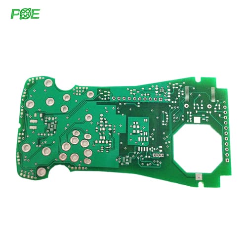
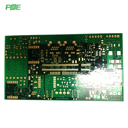
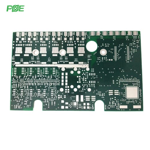
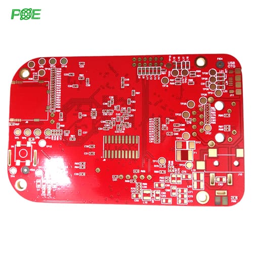
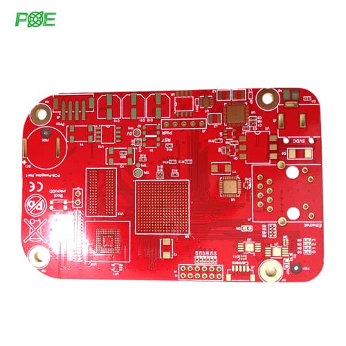
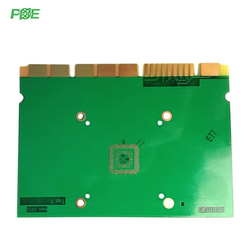
Multilayer PCB
POE Multilayer PCB Manufacturing Capabilities
No moq, 24-hour technical support;
Fast flexible PCB prototype in 3-5 days;
1-500,000 batches available, best factory price;
Free DFM (Design for Manufacturing) check
Fast quotation and reply within 4 hours
Quantity
-
+
Skype:poepcba
Whatsapp: 85292069596
Files (zip or rar files accepted. Max 8MB.)
Link Us on