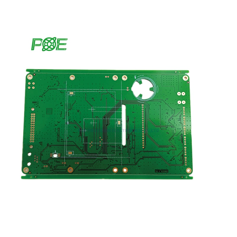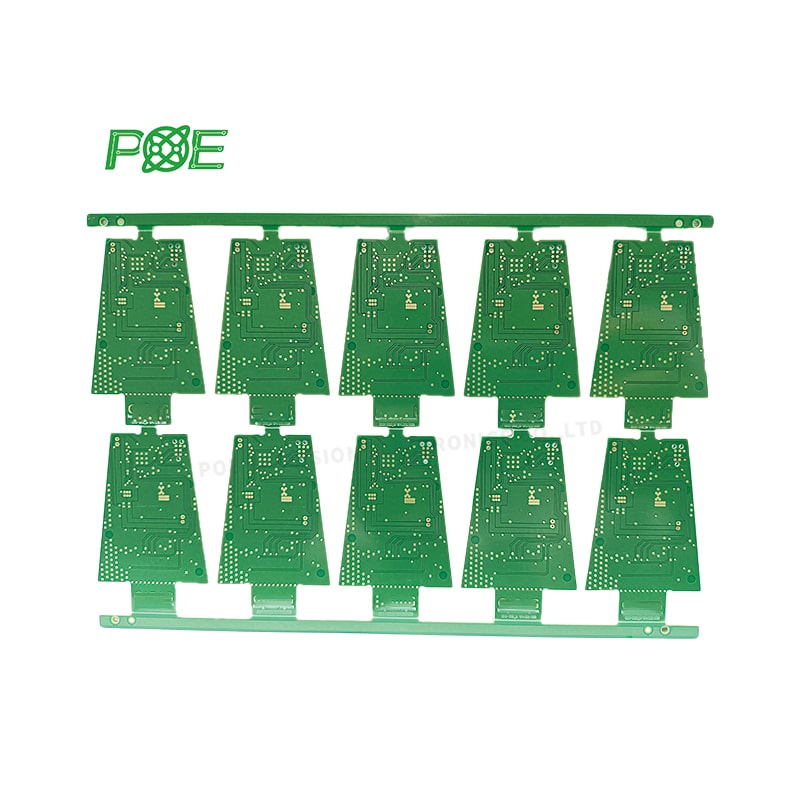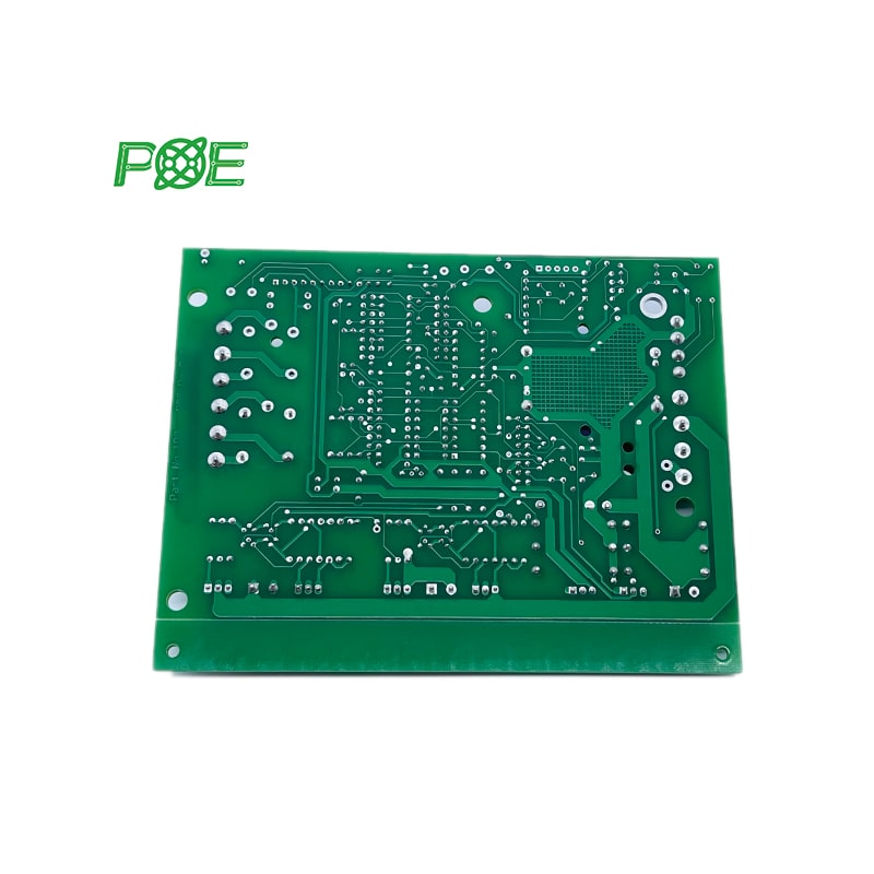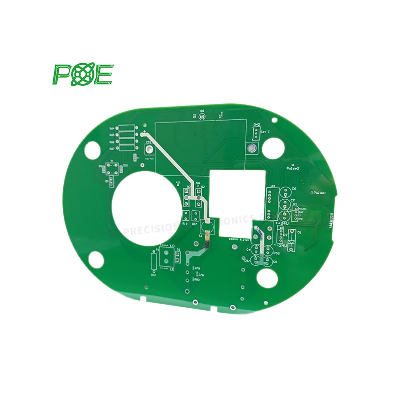
POE MANUFACTURING
YOUR GLOBAL TECHNOLOGY
PARTNER
1.Material
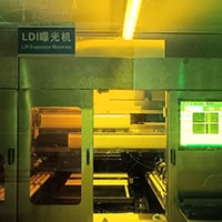
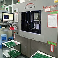
2.Inner layer Exposure
3.Inner Layers Dry film imaging
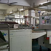
4.Inner Layers Etching
5.Inner Layers Inspection (AOI)
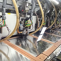
6.Brown
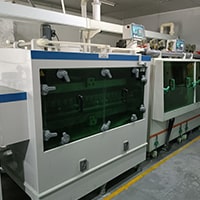
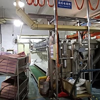
7.Lamination Layerstack
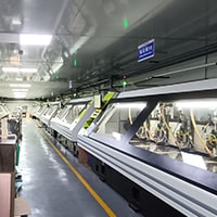
8.Lamination
9.Drilling
10.Drilling
11.Film Drop
12.PTH
13.Outer Layers Dry film imaging
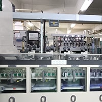
14.Copper Plating (PTH)
15.Outer Layers Etching
16.Outer Layers Inspection (AOI)
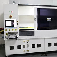
17.Inner circuit Xray
18.Soldermask
19.Solder Mask
20.Silkscreen
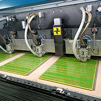
21.CNC outline
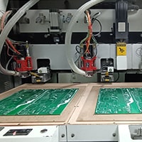
22.CNC outline
23.CNC outline
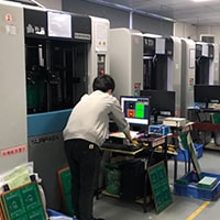
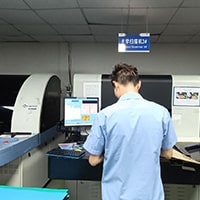
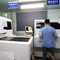
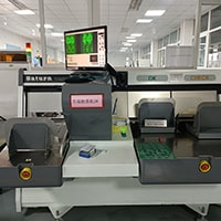
24.Probeflying
25.Probe-flying test
26.FQC Automatic
27.Automatic Etest
28.E-TEST and Probe-flying test
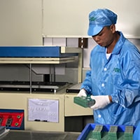
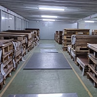
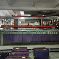
29.Vacuum Package
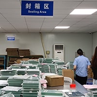
30.Vacuum package

*If you need bare PCB manufacturing + component assembly, then you need to provide gerber file and BOM.
A: Your files are held in complete safety and security. We protect the intellectual property for our customers in the whole process. All documents from customers are never shared with any third parties. We are willing to sign NDA effect by customer side local law and promising to keep customers data in high confidential level.
A: Yes.
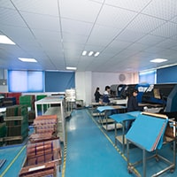
A: Yes, we are open and transparent on each production process. We Welcome you visit our factory to inspect our production process.
A: Yes, for any quality problems will take our responsibility to solve it for you any time.
A: T/T, L/C, Western Union, Paypal, Ali Pay, Credit Card.
A: 99% on-time delivery time. PCB samples are usually 5-10 days, mass production is 10-15 days, if you need to expedite, it can be shortened to 1-7 days. For some special cases, we can also notify customers in advance to avoid any accidents or losses on the customer side.

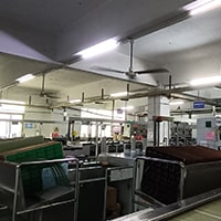
Since 1996, POE has become a globally renowned PCB company, providing small to medium volume PCB/ PCBA manufacturing services.