This website uses cookies:
Our website use cookies to analyze website accesses and improve your online experience. By continuing browsing this website,you agree to our use of cookies and privacy policy.
Accept all cookies
This website uses cookies:
Our website use cookies to analyze website accesses and improve your online experience. By continuing browsing this website,you agree to our use of cookies and privacy policy.
Accept all cookies

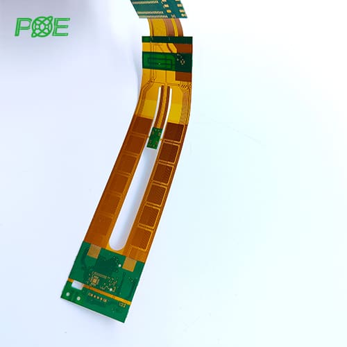
Rigid-flex PCB

Rigid-flex PCBs are used in applications where flexibility, space constraints or weight reduction are critical. Common in industries such as aerospace, automotive, consumer electronics, medical devices, and telecommunications systems.
Rigid-flex PCB
PCB Products
Description What POE Do
Description
Expanded View
Specification
Details
Layers
1-6 layers (flex area) and up to 20
Material
Polyimide, FR-4, and FR-4 High-Tg
Board Thickness
Flexible area: 0.05mm – 0.3mm, Rigid area: 0.5mm – 3.2mm
Copper Thickness
1/3 Oz (12 µm) – 2 Oz (70 µm), depends on design and material requirements
Minimum Trace Width/Spacing
3mil/3mil (0.0762mm/0.0762mm) or better, depending on design and materials
Minimum Hole Size
0.2mm (8mil) or larger, depending on layer count
Aspect Ratio
10:1 or better
Max Board Size
400mm x 500mm
Surface Finish
ENIG, Immersion Silver, OSP, HASL, Lead-Free HASL, etc
Solder Mask
Green, Blue, Yellow, Black, Red, White, and other colors
Solder Mask Resolution
4mil (0.1mm) minimum
Solder Mask Registration
±2mil (±0.0508mm)
Silkscreen Color
White, Black, Yellow
Coverlay
Polyimide, with or without adhesive, depending on the application requirements
Plated Through Holes (PTH)
Yes
Blind & Buried Vias (BBV)
Yes
Controlled Impedance
Yes, can be achieved in both rigid and flexible areas
Stiffeners
FR-4, Polyimide, or Stainless Steel, installed to provide support and rigidity when needed
Electrical Testing
Continuity & isolation, impedance control, Hi-Pot, etc.
Mechanical Assembly
Supported
Certification
ISO9001:2015;ISO13485:2016;ROHS,UL 94v0, IPC-600G classll and IPC-6012B classll standard

Purpose: To assure normal production of mutilayer pcb layer stack
If the customer has a stack up, we try to make it according to the customer's stack up.
If the customer has no overlapping structure, we will sugg-est customer to manufacture the muti-layer PCBs according to our material selection.


  • pcb layer stack
Definition
  • Core: also called copper clad laminate, has two types: single-sided copper foil or double-sided copper foil.
  • PP: Prepreg, is used to bond the copper foil and the core in the lamination process.
  • Dielectric thickness: the thickness between copper layers is called dielectric thickness, the thickness of PP after lamination, and the thickness of core plate minus copper thickness.
  • Base copper thickness: the copper thickness before production, the copper foil used for pressing and the copper thickness of the inner core plate are all called base copper thickness (if there are special processes such as thick copper 2oz ,3oz,4oz, it will be quoted separately).
  • Finished copper thickness: the copper thickness of the finished product after production, the thickness of the finished product such as the inner layer after grinding and the outer layer after electroplating surface treatment.
  • Flowing glue: In the layer press process, the thickness reduction for filling the gap between the circuit layer and PP is called flowing glue.
  • Press-fit thickness: The thickness after press-fit and before electroplating is the plate thickness without electroplating, solder resist and surface treatment.
  • Finished thickness: The thickness of finished products, but pay attention to the measuring position of board.
Laminated structure calculation rules
A: Innerlayer core thickness (copper excluded)
B: PP thickness
E: Inner copper foil thickness
F: Outside layer copper foil thickness
X: Finished board thickness
Y: Finished board thickness tolerance
Dfinition of PP: Prepreg, which consists of glass fiber and resin
Definition of PP:

Film type Glue(%) Glue flow(%) Gel time(Sec) Dielectric constant(1MHZ) PP thickness(MIL)
1080 65 35+/-5 155+/-20 3.9 2.8+/-0.5
2116LR 53 26+/-3 140+/-20 4.3 43+/-0.5
2116 55 26+/-3 140+/-20 4.25 45+/-0.5
2116HR 58 26+/-3 140+/-20 4.2 5.0+/-0.5
7628LR 43 22.5+/-5 125+/-20 4.6 7.0+/-0.8
7628 45 22.5+/-5 125+/-20 4.5 7.5+/-0.8
7630HR 50 32+/-5 130+/-30 4.4 8.5+/-1.0

Precautions
  • You can press 3 PP sheets at most.
  • Thick copper plates over 2oz cannot use single PP sheet.
  • Inter-flow glue of PP: The original thickness of PP will be reduced after pressing, mainly because the glue between PP and PP will be lost.
  • Try not to stack 3 PP sheets, which will easily lead to problems in the alignment of the board and leading to the scrapping of the board

Technology need Rigid-flex PCBs

The Rigid-flex PCB is light, thin and compact, especially suitable for the latest portable electronics and high-end medical and military equipment.
Technology need Rigid-flex PCBs

Manufacturing threshold

Because Rigid-flex PCB is mostly used in medical and military equipment, it has the strongest protection ability for products which used in harmful environment, it requires the products itself must have both the durability of PCBs and the adaptability of FPCs.

Wide range of applications, large market demands

Rigid-flex PCBs are mainly used in consumer electronics, medical machinery, military equipment, automotive electronics, precision instruments, aerospace, robots and other purposes.
Wide range of applications, large market demands

Rigid-flex PCB Technic flow and control points


Rigid-flex PCB Technic flow and control points
What POE Do

What We Can Do for You?


PCB prototype

PCB Manufacturing

☞ Turnaround time: 1-4 days;
☞ 1-6 layers(flex area) and up to 20

Small to Medium Volume;
Rigid-flex PCB;
☞ Lead Free ROHS compliant.

PCB manufacturing

PCB Assembly

☞ Lead Time: 1-7days;
Global Sourcing of Components;
Full turnkey, partial turnkey;

☞ X-ray, AOI, function test;

☞ Lead Free ROHS compliant.


Placeholder Image
  • Send gerber file to all@poe-pcba.com;
  • Get a free quote within 24 hours
  • Confirm PO from Customer;
  • DFM checking and send engineering questions (EQ);
  • Start Production, Prototype 1-4 days depending on layers;
  • Production 1-15 days depending on quantity;
  • Worldwide Shipping door to door;
  • Feedback from Customers, Order complete.


*If you need bare PCB manufacturing + component assembly, then you need to provide gerber file and BOM.

A: Your files are held in complete safety and security. We protect the intellectual property for our customers in the whole process. All documents from customers are never shared with any third parties. We are willing to sign NDA effect by customer side local law and promising to keep customers data in high confidential level.

A: Yes.

A: Yes, we are open and transparent on each production process. We Welcome you visit our factory to inspect our production process.

A: Yes, for any quality problems will take our responsibility to solve it for you any time.

A: T/T, L/C, Western Union, Paypal, Ali Pay, Credit Card.

A: 99% on-time delivery time. PCB samples are usually 5-10 days, mass production is 10-15 days, if you need to expedite, it can be shortened to 1-7 days. For some special cases, we can also notify customers in advance to avoid any accidents or losses on the customer side.

Rigid-flex PCB
Rigid flex PCB
layers: 1-6 layers (flex area) and up to 20
Copper Thickness: 1/3 Oz (12 µm) – 2 Oz (70 µm);
Certificaton: ISO9001:2015;ISO13485:2016;ROHS,UL 94v0, IPC-600G classll and IPC-6012B classll standard;
Quantity
-
+
Skype:poepcba
Whatsapp: 85292069596
Files (zip or rar files accepted. Max 8MB.)
Link Us on