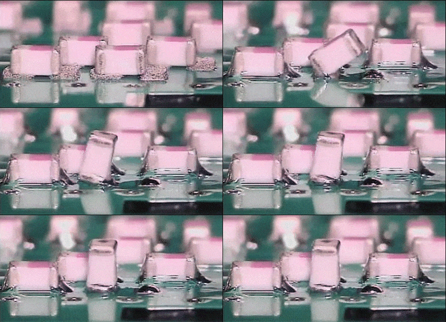
Why is there PCB Tombstone in SMT?
21 January 2025
Views: 1569
What is pcb tombstone?
PCB tombstone is also called PCB Manhattan phenomenon. PCB tombstone refers to components (often occurring in chip capacitors and chip resistors, especially 1005 or smaller 0603 chip components) that after SMT welding, one end leaves the pad while the other end is still connected to the pad. This causes the components to appear perpendicular to the PCB.
Why does pcb tombstone occur?
1.Material issues
This is the most basic problem. PCB tombstone phenomenon will occur when the solderability of the two soldering terminals of the component is poor.
2. Pad design
2.1 The spacing between the pads is too large. Excessive spacing between the two pads will cause the components to shift and separate from the solder paste when the solder wets the component terminals.
2.2 The pad size is inconsistent and the heat capacity is different
The areas of the welding areas of the two pads are different. The upper pad is made of solder mask windows on a large piece of copper foil, so it is larger than the lower pad. The upper pad is connected to a large piece of copper foil, and the heating rate during reflow is smaller than that of the lower pad. The different melting and wetting rates of the solder paste cause the phenomenon of PCB tombstone, especially for 1005 or smaller 0603 chip components. .
2.3 PCB tombstones caused by solder mask are rare. If it does occur, it can be solved by removing the solder mask between the pads.
3. Process design
3.1 The solder paste printing is offset. In order to avoid the problem of solder beads when opening the stencil and increase the spacing between the pads, the probability of PCB tombstone after reflow will be greater.
3.2 Mounting misalignment means component misalignment, resulting in insufficient contact between the welding terminals and the solder paste, resulting in uneven wetting or wetting force. This requires optimizing the mounting procedure.
3.3 Nitrogen is an inert gas that can isolate the influence of oxygen, thereby improving the solderability of solder terminals and the wettability of solder paste, as well as the ability of solder paste to melt on PCB pads and component terminals. This is a very good design when operated properly, but if there is a difference in the solderability of the two terminals of the component, nitrogen will increase this difference, so when the nitrogen concentration is high and the oxygen concentration is below 1000PPM, PCB problems will occur. Tombstone situation.
3.4 Improper configuration file settings
During reflow, if the heat difference on the PCB is large, causing thermal shock and causing the temperature to rise too fast, the phenomenon of PCB tombstone may occur. Generally, the temperature rise slope should not exceed 2°C per second, and try to keep the PCB temperature balanced before reflow.
Conclusion
The appearance of pcb tombstone after SMT processing has a great impact on product quality and repair costs. Improving and optimizing the detection and processing processes can make production smoother.


