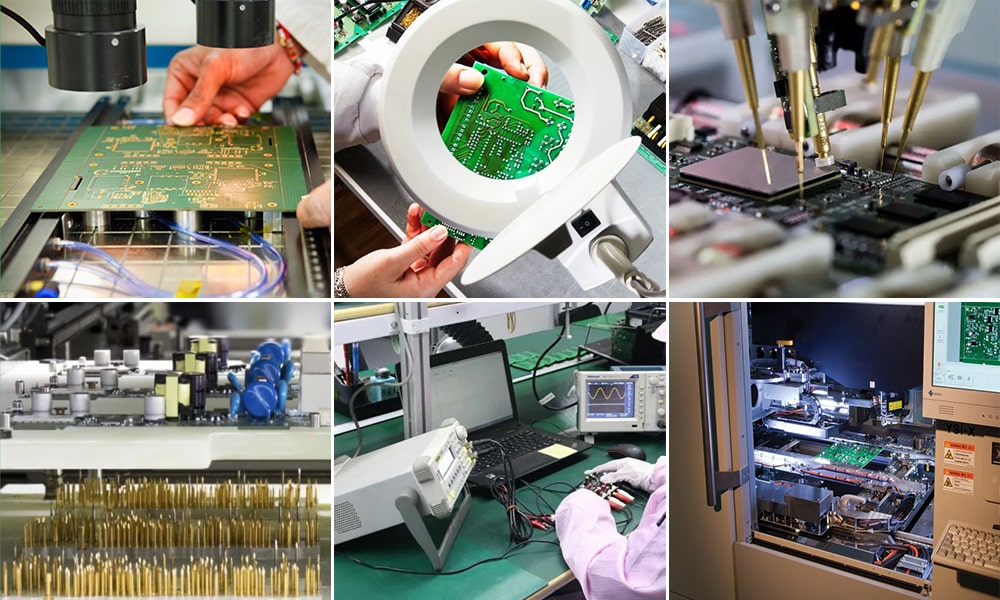
What tests does PCB manufacturing need to go through?
20 January 2025
Views: 783
Testing during the PCB manufacturing process is essential to ensure the quality of the final finished PCB. The main tests are

1. Bare board test
The first test after PCB manufacturing before assembly to verify basic integrity, open circuits, short circuits and correct connections between points.
2. Visual inspection
Visual inspection can be manual or automatic using AOI (automatic optical inspection).
It can detect easier problems such as drilling, copper wire quality, solder mask, screen printing quality or surface defects.
3. Flying probe test
Use moving probe to check electrical connections, which is more flexible than fixture testing and is very suitable for prototypes or small batch production.
4. In-circuit test (ICT)
ICT is performed after PCB assembly. It uses a "bed of nails" fixture to contact the test points simultaneously. It mainly tests components, solder joint quality and circuit function.
5. Functional test
Functional test can ensure that the product can operate normally, including power-on test, signal output test, circuit performance test, environmental test, load test.
6. X-ray inspection
X-ray testing is important for multi-layer boards and BGA components. It can detect whether the internal layers are aligned, hidden solder joints, void detection, and component placement
These tests can ensure that the PCB meets quality standards after manufacturing. However, tests need to be performed according to different needs, and not all tests need to be performed.
Share This Story, Choose Your Platform!


