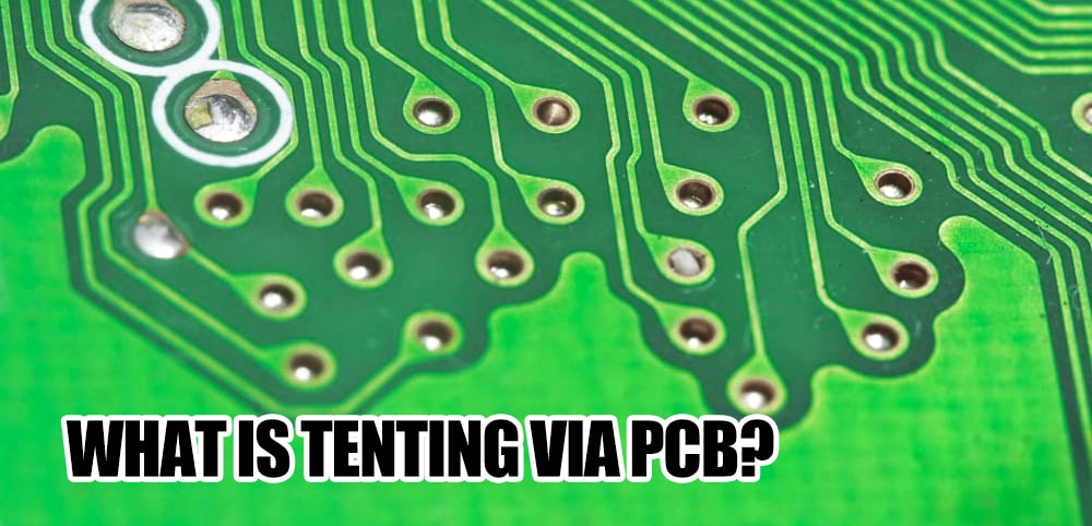
What is tenting via PCB?
Vias are small holes in a PCB used to provide interconnections between different layers. Electroplating is used to increase conductivity within the through holes to enable signal conduction between different layers. However, the impact of leaving the via completely exposed is significant, so the via requires some method of handling. There are currently two main methods to deal with through holes: one is the filling through hole method, which uses non-conductive material to fill the inside of the through hole; the other is the tenting via method, which uses a solder mask coating to cover the annular area around the through hole, leaving the through hole The internal pathway is called tenting via PCB.

Tenting via PCB can better conduct electrical signals. In areas with dense SMT pad layout, using tenting via can prevent short circuit problems caused by components touching the edges of through holes. Compared with the method of completely closing the through hole, tenting via can ensure that the through hole is unobstructed without additional processing. It is the most widely used method at present.
At POE, we can have rich experience in all types of PCBs, develop different manufacturing plans according to customers' unique needs, and help achieve the best quality PCBs. Leave a message to contact us to get started!
Share This Story, Choose Your Platform!


