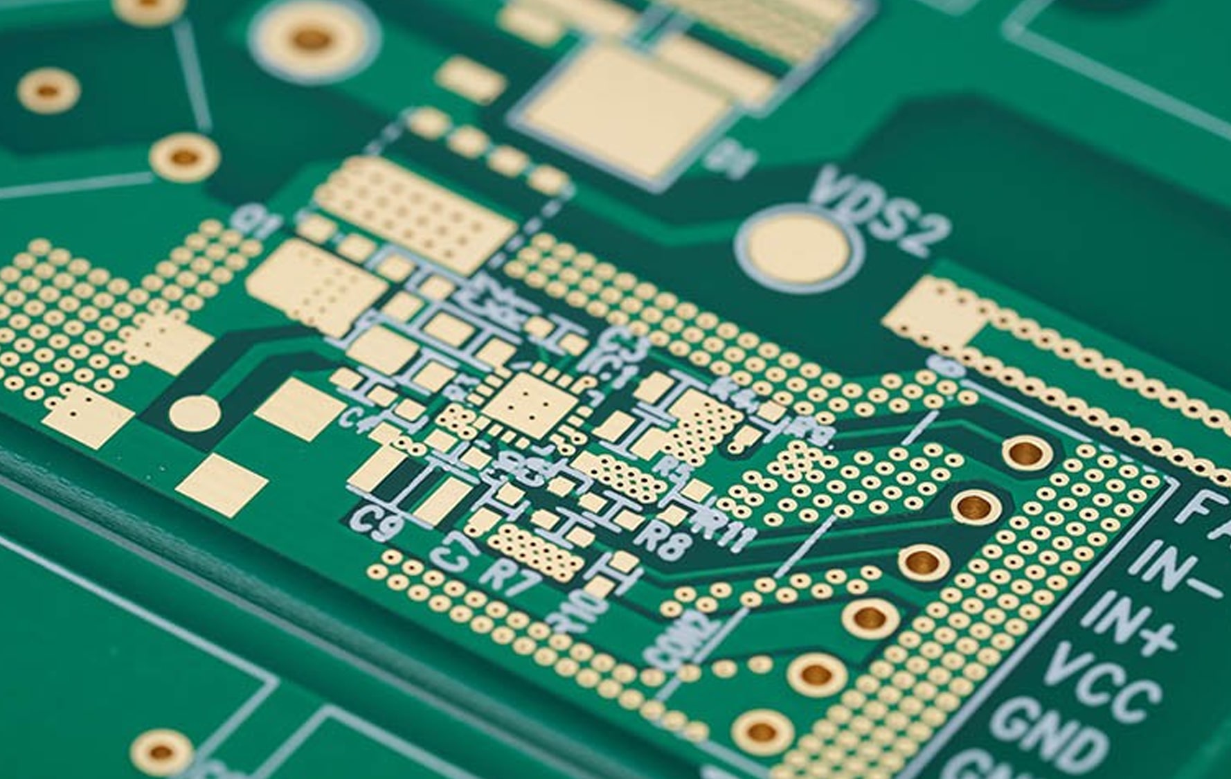
What is PCB OSP surface treatment?
22 January 2025
Views: 101
One of the key steps in PCB manufacturing is surface treatment, which can protect the exposed copper on the circuit board and prepare it for soldering. Among the various surface treatment methods, OSP is one of the most popular methods.

What is OSP surface treatment?
OSP is the abbreviation of organic solderability preservative, which is a surface treatment process for PCBs to protect the exposed copper pads from oxidation. Copper will corrode when exposed to air. OSP applies a thin organic protective layer on the copper to prevent copper oxidation while still allowing the copper to maintain its excellent solderability.
How does OSP work?
The OSP process is to apply a water-based organic compound to the copper pad of the PCB. The organic compound combines with the copper to form a very thin and transparent protective film. Meaning that it will not interfere with subsequent soldering. When soldering begins, the OSP layer dissolves, exposing the clean copper underneath, allowing the solder to bond.
Advantages of OSP
Environmental protection: OSP is a lead-free and environmentally friendly process. There are no toxic chemicals and heavy metals, which is an ideal choice for environmentally friendly manufacturing.
Cost-effectiveness: OSP is inexpensive compared to other surface finishes such as ENIG (Electroless Nickel Immersion Gold) or HASL (Hot Air Solder Leveling).
Good Solderability: OSP maintains excellent assembly solderability, ensuring strong and reliable solder joints.
Simple Process: OSP process is simple and does not require complex machinery.
Disadvantages of OSP
Limited durability: The organic layer is thin and will degrade over time.
Not suitable for multi-layer boards: OSP is best suited for single or double-layer PCBs.
Fragile: OSP layers are brittle and can wear away if the PCB is handled roughly or exposed to contaminants.
When to use OSP?
Cost-sensitive projects: When cost is the main consideration, OSP is an excellent choice due to its affordable price.
Short production cycle: OSP can be very effective for products with short turnaround times.
Simpler PCBs: Single or double-layer boards benefit the most from OSP.
If your product requires high durability, long-term storage, or exposure to harsh environments, other surface finishes such as ENIG or HASL may be more suitable.
Conclusion
OSP is a simple, cost-effective and environmentally friendly surface finish for protecting PCB copper pads. Suitable for projects with low budgets and short production cycles.


