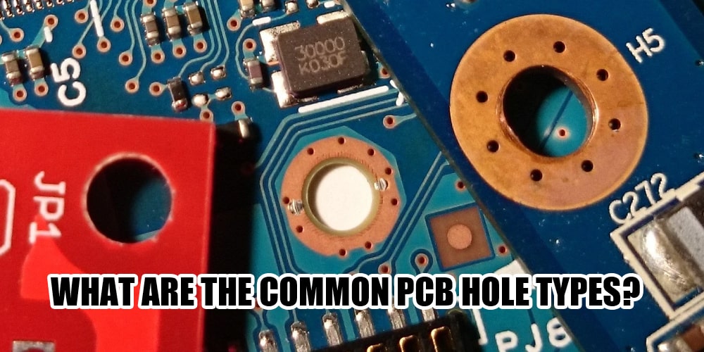
What are the common PCB hole types?
20 January 2025
Views: 1081
PCB hole is one of the important features for connecting PCB components. Common PCB hole types mainly include through hole, countersunk hole, blind hole, micro hole, etc.
Through Hole
Used to install traditional Through Hole components, such as resistors, capacitors, etc., which need to pass through from one side to the other. Connect the conductive routes between different layers of multi-layer PCB.
1. Exceeding 1.0mm, the diameter is generally 1.0~5.0mm.
2. Punching to install large components such as IC pins or resistors, with pads on both sides.
3. Strong accommodation, suitable for large-size components; simple processing.
4. Occupies a large PCB area.
Plated Through Hole
Applications that require opening a hole on one side of the PCB without passing through to the opposite side. Often used when installing surface mount components (SMD), such as IC chips, CCD image sensors, etc.
1.0.4~1.0mm, the thin sheet can be as small as 0.3mm.
2. Install SMD components or circuits.
3. Save area; component installation is less difficult.
4. The manufacturing process is complex and the size of the components is limited.
Blind Hole
It is used to connect the internal wires of different layers in multi-layer PCB. It is used in the inner layer of PCB but not directly exposed on the surface of PCB.
1. Diameter 0.2~1.0mm, depth ≤ half of the PCB thickness.
2. Embed components or increase the number of PCB layers.
3. Save more area; the component installation is well concealed.
4. Difficult to process; difficult to locate.
Microvia Hole
It is used to connect very fine inner layer leads in modern high-density PCB boards, such as very fine signal lines. The size of microvia is generally less than 0.3mm.
1. Diameter ≤100um, used for high-density PCB.
2. Connect inner layer lines or increase the height of SMD pads.
3. Extremely save area; increase PCB fixed point density.
4. High manufacturing cost; extremely difficult to locate.


