Our website use cookies to analyze website accesses and improve your online experience. By continuing browsing this website,you agree to our use of cookies and privacy policy.
Accept all cookies
Decline
This website uses cookies:
Our website use cookies to analyze website accesses and improve your online experience. By continuing browsing this website,you agree to our use of cookies and privacy policy.
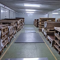
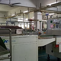
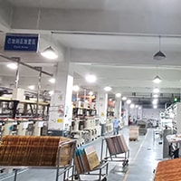
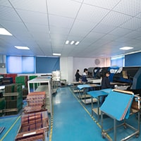
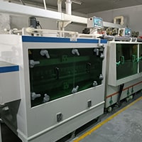
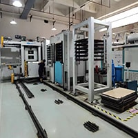
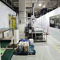
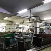
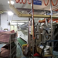
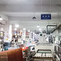
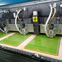
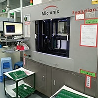
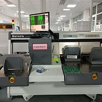
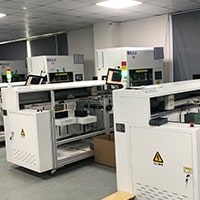
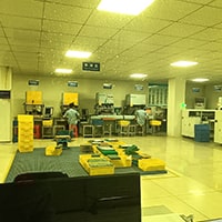
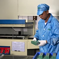
PCB manufacturing is a complex process, and the correct implementation of each step can ensure the quality of the finished product. Below we have detailed the 26 steps of manufacturing PCBs. Together, they transform raw materials into PCBs.
Video of PCB manufacturing steps:
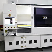
1. Materials
PCB manufacturing begins with selecting the substrate for the PCB. It is usually made using fiberglass (FR4), copper foil, and resin.
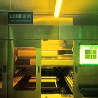
2. Inner Layer Exposure
The inner copper layer is ready to form the circuit. A photosensitive dry film is laminated onto the copper surface, which will later define the circuit pattern of the PCB.
3. Inner Layer Dry Film Imaging
The dry film is exposed to ultraviolet light through a photomask, which hardens the exposed areas to form the desired pattern. The unhardened areas are washed away to reveal the copper underneath.
1.Material
2.Inner layer Exposure
3.Inner Layers Dry film imaging
4. Inner Layer Etching
A chemical etch is used to remove the exposed copper, leaving only the circuit pattern defined by the hardened dry film. After etching, the dry film is peeled off, leaving a clean copper circuit.
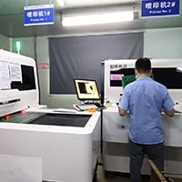
5. Inner Layer Inspection (AOI)
Automated Optical Inspection (AOI) checks inner layers for defects such as shorts or opens, ensuring that inner layers are defect-free before further processing.
6. Brown Oxide Treatment
Chemical treatment of inner copper layers to create a rough surface that improves adhesion during lamination.
4.Inner Layers Etching
5.Inner Layers Inspection (AOI)
6.Brown
7. Laminate Layer Stacking
Inner layers are stacked together with prepreg and copper foil to create the desired layer structure. They will be bonded together in the next step.
8. Lamination
The stacked layers are pressed and heated in a laminator, bonding them into a single, solid PCB panel, ensuring proper alignment and mechanical strength.
9. Drilling
Hole drilling is done in PCBs to create channels for electrical connections and mounting points. These include through-holes, blind vias, buried vias, and other types of holes, depending on the design.
7.Lamination Layerstack
8.Lamination
9.Drilling
10. Deburring and Hole Cleaning
After drilling, the holes are cleaned to remove debris and burrs. This ensures proper plating and functionality in subsequent steps.
11. Thin Film Dispensing
A photosensitive film is applied to the outer layers of the PCB in preparation for circuit patterning, defining the outer circuitry of the PCB.
12. PTH (Plated Through Hole)
A thin layer of copper is plated over the drilled holes through a chemical deposition process, creating electrical connections between the layers of the PCB.
10.Drilling
11.Film Drop
12.PTH
13. Dry Film Imaging of the Outer Layers
Similar to the inner layers, a dry film is applied to the outer layers and exposed to UV light through a photomask, defining the circuit pattern of the outer layers.
14. Copper Plating (PTH)
The outer layer circuits are reinforced with an additional layer of plated copper, ensuring good conductivity and durability.
15. Etching of the Outer Layers
The exposed copper on the outer layers is chemically etched away, leaving the desired circuit pattern. The dry film is then removed.
13.Outer Layers Dry film imaging
14.Copper Plating (PTH)
15.Outer Layers Etching
16. Inspection of the Outer Layers (AOI)
The outer layers are inspected using AOI to detect any defects in the circuit pattern, ensuring the integrity of the outer circuitry.
17. Internal Circuit X-ray Inspection
X-ray inspection is performed to verify the alignment of inner and outer layers, ensuring that all layers are properly registered.
18. Solder Mask Application
Solder mask is applied on PCBs to protect the copper circuits from oxidation while preventing solder bridging during component assembly.
16.Outer Layers Inspection (AOI)
17.Inner circuit Xray
18.Soldermask
19. Solder Mask Imaging
The solder mask is exposed to UV light through a photomask, which defines the soldering areas. Unexposed areas are washed away.
20. Silkscreen Printing
Silkscreen layers are used to print labels, logos, and other markings on PCBs, which help identify components and test points during assembly.
21. CNC Contour Milling
The PCB is cut to final size and shape using a CNC machine, this step defines the outline of the board and creates any slots or cutouts.
19.Solder Mask
20.Silkscreen
21.CNC outline
22. Flying Probe Testing
The flying probe tester checks the electrical connectivity of the PCB by probing various test points. This ensures that all circuits are functioning as expected.
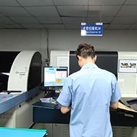
23. Final Quality Control (FQC)
Automated systems and human inspectors perform final quality checks on PCBs to ensure that the boards meet all specifications and standards.
24. Automated Electrical Test (E-Test)
PCBs are electrically tested to verify that all circuits are complete and functional. This test checks for shorts, opens, and other problems.
22.Probe-flying test
23.FQC Automatic
24.Automatic Etest
25. E-Test and Flying Probe Retest
If there are any issues If problems are found in the initial test, the PCBs are retested using flying probes and electrical test equipment to confirm the results.
26. Vacuum Packaging
Finally, the PCBs are vacuum sealed to protect them from moisture and contamination during transportation and storage. The boards are then ready for delivery to customers.
25.E-TEST and Probe-flying test
26.Vacuum Package
Conclusion
The PCB manufacturing process is a meticulous and multi-step operation that requires precision and accuracy at every stage. Each step plays a critical role in ensuring that the final product meets the design specifications.
POE can quickly provide you with PCB prototype/ small and medium-volume PCB/ PCBA manufacturing. Send your PCB files or BOM list to us and you will get a quote as soon as possible!