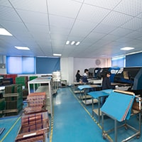
PCB Fabrication and Assembly Process
20 February 2025
Views: 286
Electronic devices need PCBs to function. The process of PCB fabrication and assembly is very complex. Here is a step-by-step explanation of PCB fabrication and assembly, so you can easily understand the entire PCB fabrication and assembly process.
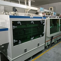
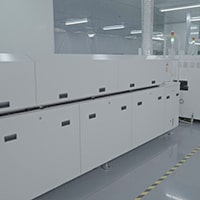
PCB Fabrication
1.Material
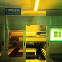
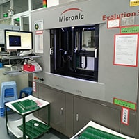
2.Inner layer Exposure
3.Inner Layers Dry film imaging
4.Inner Layers Etching
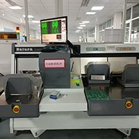
5.Inner Layers Inspection (AOI)
6.Brown
7.Lamination Layerstack
8.Lamination
9.Drilling
10.Drilling
11.Film Drop
12.PTH
13.Outer Layers Dry film imaging
14.Copper Plating (PTH)
15.Outer Layers Etching
16.Outer Layers Inspection (AOI)
17.Inner circuit Xray
18.Soldermask
19.Solder Mask
20.Silkscreen
21.CNC outline
22.CNC outline
23.CNC outline
24.Probeflying
25.Probe-flying test
26.FQC Automatic
27.Automatic Etest
28.E-TEST and Probe-flying test
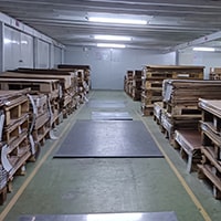
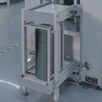
29.Vacuum Package
30.Vacuum package
1. Design and Layout
The first step in PCB fabrication is to use professional software such as Altium Designer, Eagle or KiCAD to design a schematic with all components and connections, and layout the board, define layers, copper wires and place components. Finally, a Gerber file containing the data required for manufacturing is generated.
2. Material Selection
PCBs are made of conductive (copper) and non-conductive (substrate, such as FR4) material layers. Including: substrate, copper foil, surface treatment.
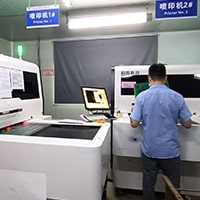
3. Printing Circuit Patterns
The circuit design is transferred to the copper clad board using a photoresist coating or laser to write the pattern directly to the circuit board.
4. Etching Copper
After printing the circuit pattern, a chemical etchant is used to remove the unwanted copper, leaving only the required copper traces. The steps include: 1. Immersing the board in an etching solution; 2. Cleaning and drying the board to remove excess chemicals.
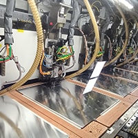
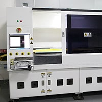
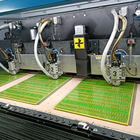
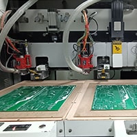
5. Drilling
Using CNC machines to accurately drill holes to create holes for electrical and mechanical purposes. Types of holes include through-holes, blind vias, buried vias, and non-copper vias.
6. Plated holes
For electrical connections, plated through holes (PTHs) are created by depositing copper onto the walls of the drilled holes. This is achieved by using chemical plating and electroplating.
7. Lamination
For multi-layer PCBs, the layers are aligned and laminated together under high pressure and temperature.
8. Surface treatment application
Exposed copper traces need to be protected from oxidation, and surface treatment can improve solderability. Common surface treatments include HASL, ENIG, OSP.
9. Solder mask application
The solder mask (usually green) is applied to the PCB, which is the color of the PCB that we can see most intuitively. It is produced in this step. To isolate the copper traces and prevent solder bridges during assembly. The solder mask is applied to all areas outside the pads.
10. Silkscreen Printing
The silkscreen layer is printed on the PCB to display text, symbols and markings for component identification and location.
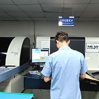
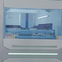
11. Electrical Testing
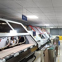
The manufactured PCB is subjected to Bare Board Testing (BBT) to ensure that all connections are correct and there are no shorts or opens. The manufacturing of the bare board PCB is now complete.
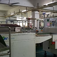
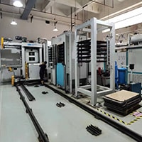
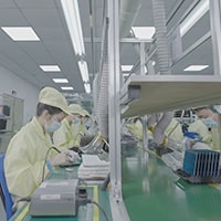
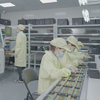
PCB Assembly
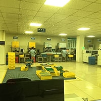
After the bare PCB is manufactured, the next step is to assemble the components onto the board. This process is called PCB Assembly (PCBA), and this step is the step that actually realizes the functionality of the PCB. Here are the detailed steps:
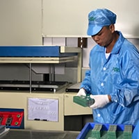
1. IQC
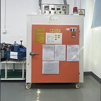
2. PCB Dry Oven
3. Automatic PCB Loader
4. Solder Paste Machine
5. SPI
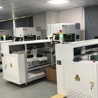
6. SMT Machine
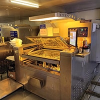
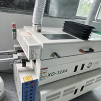
7. Nitrogen Reflow Oven
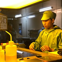
8. Manual Soldering
9. DIP Lines
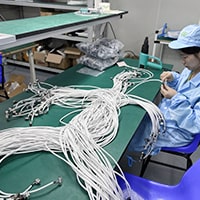
10. Cable Assembly
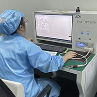
11. FAI
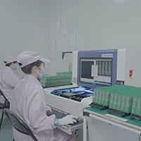
12. QC
13. PCBA Clean Washer
14. Program And Testing
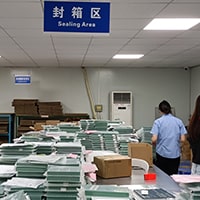
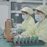
15. Packaging
1. Procurement of Components
The required components will be procured according to the design files to assemble the PCB.
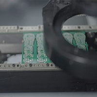
2. Solder Paste Application
Surface mount components require solder paste to be applied to the PCB pads using a stencil to ensure precise placement and secure connections.
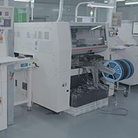
3. Component Placement
The components are placed on the PCB using manual placement (commonly used for prototypes) or a pick and place machine.
4. Soldering
Soldering fixes the components on the PCB. Common ones are reflow soldering and wave soldering.
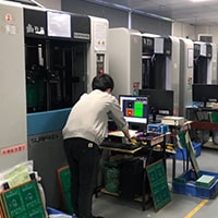
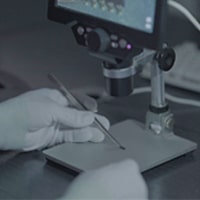
5. Inspection and testing
After soldering, components are inspected for defects and tested for functionality, including automated optical inspection (AOI), X-ray inspection, circuit testing (ICT), functional testing.
6. Cleaning
After assembly, PCBs are cleaned to remove flux residues or contaminants that may affect performance.
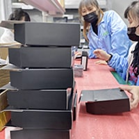
7. Packaging and delivery
Once the PCBs pass all inspections, they are packaged and shipped to customers for integration into the final product. At this point, PCB fabrication and assembly are completed smoothly.
Conclusion
PCB fabrication and assembly are detailed processes that require precision, quality control, and advanced technology. From designing the circuit board to assembling the components, every step is important.