PCB Edge Design for SMT Assembly
21 January 2025
Views: 1190
During SMT patch processing, the PCB is transported through the guide rail, so the forbidden area must be reserved on both sides of the PCB as the transmission edge. Usually, the long side of the PCB or the large board after assembly is used as the transmission edge.
The fixed plate width of the SMT transmission track is 3.0mm. Although the theoretical limit of the transmission edge is also 3.0mm, in order to avoid increasing the difficulty of patch processing, it is recommended to reserve more space and use 5.0mm as the forbidden area of the transmission edge.
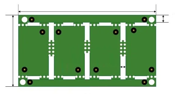
If the forbidden area is not enough, when the PCB is placed on the transmission rail, the interference part may affect the solder paste or the placed components. At this time, the interference part can only be post-soldered or a separate fixture is required, which increases the production cost. If the distance between the patch component in the board and the board edge is far enough and not within the track range, no additional process edge is required; if the component is within the track range, a process edge must be added as a clamping edge area. The width of the process edge generally requires 3-10mm according to the characteristics of the machine, and 5mm is the most common.

Usually, the process edge is added on the longer side so that the board enters the SMT machine vertically. In this way, the hardness of the board is higher and it will not bounce due to the light pressure of the machine probe during patching. However, the longer process edge will increase the average price of a single board. If the hardness of the board is sufficient, the process edge can be added in the short side direction, so that the process edge area is smaller, the average cost of a single board is lower, and the board enters the SMT machine horizontally.
SMT usually uses MARK points for alignment. If there is no MARK point in the board, 2-4 MARK points must be added diagonally on the process edge. The size is generally 1.0mm, and the copper is exposed and tinned. If there is a MARK point in the board, the process edge can be added or not.
In the production process of the board factory, molding and testing require positioning, so adding special positioning holes to the process edge can make the appearance more standard and positioning more convenient. Usually, 3-4 positioning holes with a diameter between 2.0-4.0mm will be added to the process edge, and the diameter of 3mm is the most common.
Obviously, the PCB in the automotive autopilot system has requirements for precision, power consumption, heat dissipation, durability and rugged reliability.
Notes on process edge design
Patches or machine-inserted components cannot be arranged in the process edge, and their entities cannot enter the process edge and the space above it.
The physical body of the hand-inserted components cannot fall within the space within 3mm above the upper and lower process edges, and within 2mm above the left and right process edges.
The conductive copper foil in the process edge should be as wide as possible. Lines less than 0.4mm need to be treated with enhanced insulation and wear resistance, and the lines on the edge should not be less than 0.8mm.
The process edge can be connected to the PCB with stamp holes or V-grooves, and V-grooves are generally used.
There should be no pads or through holes on the process edge.
Single boards with an area greater than 80mm² require the PCB itself to have a pair of parallel process edges, and no physical components enter the space above and below the process edges.
The width of the process edge can be appropriately increased according to actual conditions.
Share This Story, Choose Your Platform!

