
POE MANUFACTURING
YOUR GLOBAL TECHNOLOGY
PARTNER
| Drilling (DR) | 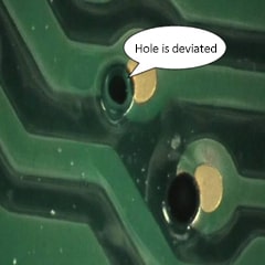 |
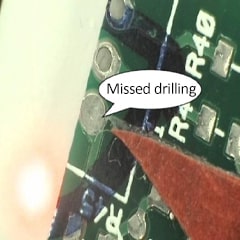
Drilling anomaly causes the hole not to be drilled to the graphic position |
| Component holes are 2mil, and via holes are allowed to be tangent; Those shown in the picture should be scrapped. |
||
 |
1. The positioning is not correct when the hole is filled after the drilling is missed; 2. The positioning is not ideal; 3. The pin hole is too large, resulting in poor fixation. |
|
| 1. Component holes are 2mil, and electrical holes are allowed to be tangent; 2. Scrap as shown in the figure. |
||
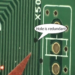 |
1. Failure to produce according to the information provided by the Engineering Department, and unauthorized changes to the information resulted in more holes than the specified number; 2. Wrong information was used. |
|
| Scrapped | ||
 |
No borehole | |
| 1, with red philine beat; 2. This drawing is not acceptable. |
||
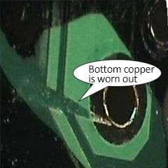 |
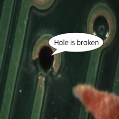
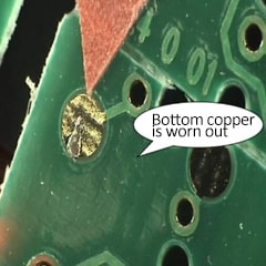
Improper operation or equipment problems cause sharp objects to hit the board surface and cause the base copper to fall off. | |
| 1. Scrap at the line bends and pads; 2. Repair the line; 3. UAI on the large copper sheet. |
||
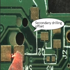 |
The positioning is not ideal, the positioning hole is larger than the pin, causing the second drill hole to deviate from the pattern. | |
| Scrapped | ||
| Copper (PTH) | 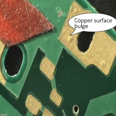 |
Electroplated copper bubbles |
| Scrapped | ||
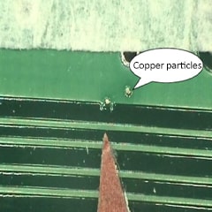 |
Copper cylinder liquid pollution, the external environment dust into the copper cylinder, resulting in granular copper on the surface. | |
| The maximum diameter of the copper particles should be less than 0.05mm, and there should be no more than 5 in every 304.8mm×304.8mm area. | ||
 |
Improper operation or equipment problems cause sharp objects to hit the plate surface and make the base copper fall off. | |
| 1. Scrap at the line bends and pads; 2. Repair the line; 3. UAI on the large copper sheet. |
||
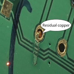 |
Copper cylinder pollution, residual copper on the surface | |
| The residual copper between the lines shall not affect the line width and spacing, and the length shall be <13mm. The residual copper on the effective plate surface shall be repaired. | ||
| Outer dry film (ODF) | 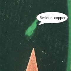 |
Residual copper |
| 1. It does not affect the line width and line spacing; 2. The residual copper on the large copper surface is allowed to be 1.0mm and the copper must not be exposed. Only one is allowed within an area of 9 square centimeters. |
||
 |
The board got stuck during the grinding process and was damaged. | |
| Scrapped | ||
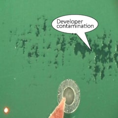 |
Developer contamination | |
| 1. 10 * 10 MM 2 on large copper foil is acceptable; 2. Not acceptable on circuits or pads. |
||
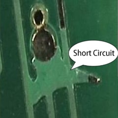 |
Short circuit | |
| Scrapped | ||
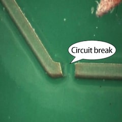 |
Poor exposure results in an open circuit. | |
| Scrapped | ||
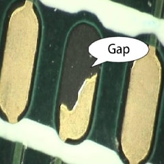 |
During the exposure process, small film fragments or other foreign matter adhere to the pad, causing gaps. | |
| 1. No gaps are allowed in IC, BGA and gold finger positions; 2. No gaps are allowed in the middle of square and round pads, but 5% is allowed around them. |
||
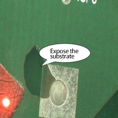 |
Expose the substrate | |
| 1. No gaps are allowed in the IC position; 2. No gaps are allowed in the middle of square and round pads, but 5% is allowed around them. |
||
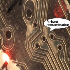 |
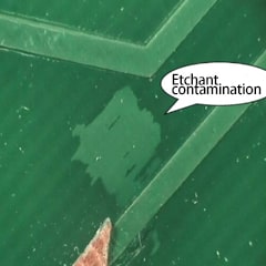
Etchant contamination | |
| Meet MI line width spacing requirements. | ||
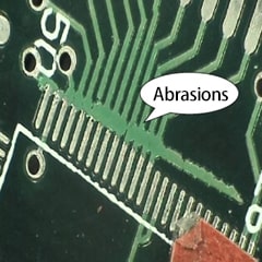 |
Scratches caused by human operation problems | |
| Scrapped | ||
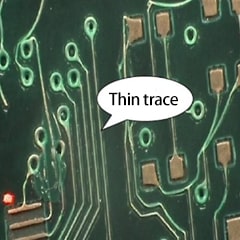 |
The etching speed is too slow, the temperature is too high, and the concentration of the solution is too high, resulting in thin lines. | |
| Within the requirements provided by the customer. | ||
 |
1. Poor etching uniformity; 2. Nozzle clogged; 3. Incorrect etching parameters. |
|
| Scrapped |

Since 1996, POE has become a globally renowned PCB company, providing small to medium volume PCB/ PCBA manufacturing services.