Industrial PCB Manufacturing
07 February 2025
Views: 108
PCBs are an important part of electronic products. They are flat plates made of non-conductive materials with a conductive copper layer etched on the surface, forming a pathway for electrical signals, allowing different components on the board to communicate and function as expected. Industrial PCB manufacturing is a highly specialized process.

Steps in Industrial PCB Manufacturing:

1. Design and Layout
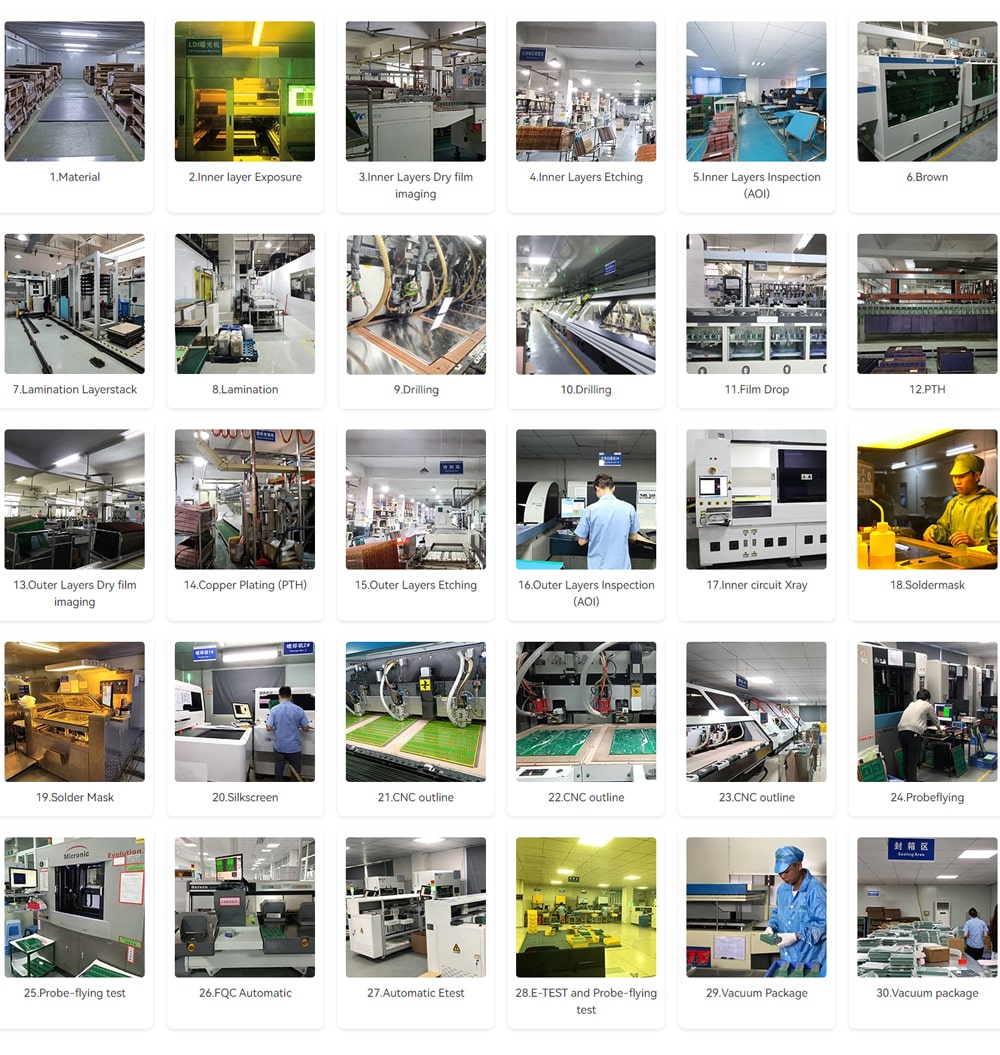
It starts with engineers designing the PCB layout using professional software such as Altium, Eagle, KiCad, etc. The design specifies the locations of components, traces, and holes required for the board to function. This design is then converted into a Gerber file, which serves as a manufacturing blueprint.
2. Material Selection
The substrate of the PCB is usually a composite material of FR4 and other non-conductive materials, which is then laminated with copper foil to form a conductive layer. The choice of material depends on the application, such as high-frequency circuits, flexible PCBs, or rigid boards.
3. Etching
The copper laminate goes through an etching process to create the circuit pattern. A layer of photoresist is applied, and ultraviolet (UV) light is used to expose the desired circuit design. The exposed areas are then chemically etched, leaving copper traces.
4. Drilling
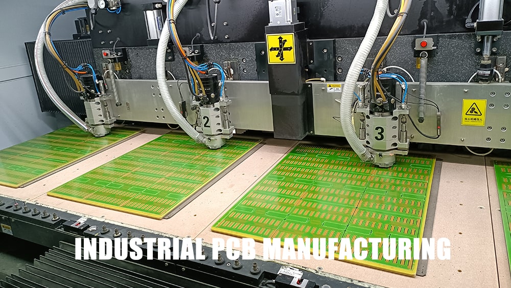
PCBs require a variety of holes for different purposes. These holes are drilled using high-precision CNC machines. Hole types include through-holes (PTH, NPTH), blind vias, buried vias, countersunk vias, locating holes, reference holes.
5. Lamination
For multi-layer PCBs, the layers are aligned and pressed together under high pressure and temperature, which ensures that the layers are firmly bonded and the circuit paths are perfectly aligned.
6. Plating
Copper plating is applied to the PTH and board surface. Copper is deposited onto the board through a chemical bath to ensure proper conductivity.
7. Solder Mask Application
A thin layer of solder mask is applied to the board to prevent oxidation and shorting of copper traces. The solder mask also defines the area where solder is applied during component assembly.
8. Silkscreen
Text, symbols, and component labels are printed onto the PCB using a silkscreen process, which helps identify components and provide assembly guidance.
9. Testing and Quality Control
Each PCB is rigorously tested to ensure that it meets design specifications and industry standards. Common testing methods include electrical testing and optical inspection.
10. Assembly
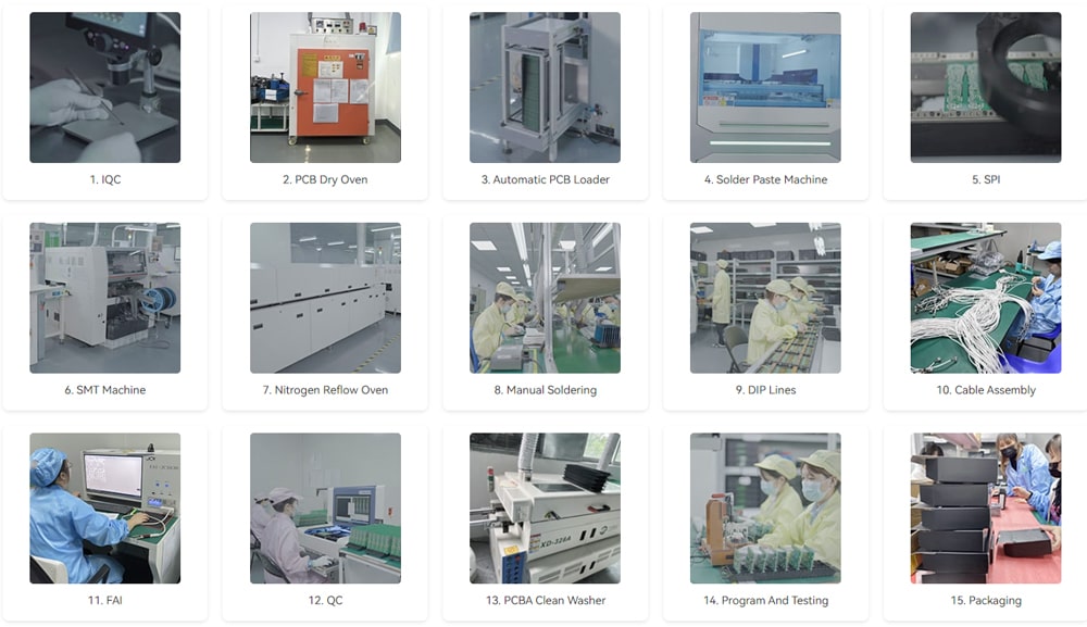
After PCB manufacturing is complete, components such as resistors, capacitors, and ICs are mounted. This is done using surface mount technology (SMT) and through-hole soldering, which gives the PCB actual functionality.

Conclusion
Industrial PCB manufacturing is a complex, multi-step process that requires precision, advanced technology, and expertise. From designing the layout to drilling different types of holes and testing the final product, each step plays a vital role in ensuring the functionality and reliability of the PCB.
