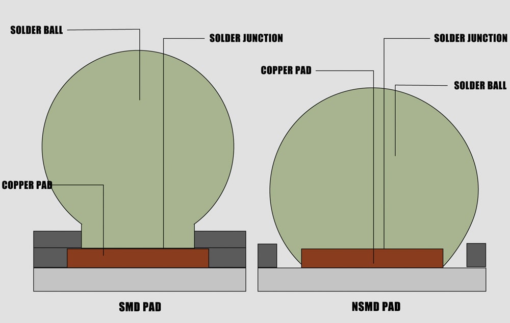
Difference between SMD and NSMD in BGA Package
22 January 2025
Views: 97
BGA package is a commonly used technology for electronic products, especially in high-density interconnection applications. In BGA, the two main pad designs of pads on PCB are SMD and NSMD.
What is SMD?
The characteristic of SMD pads is that the solder mask overlaps the edge of the copper pad, and the solder mask defines the size of the pad. The copper area under the solder mask is slightly larger than the opening in the solder mask, forming a boundary that limits solder paste and solder balls during the reflow process.
Main characteristics of SMD pads
Solder mask overlap: The solder mask partially covers the edge of the copper pad, reducing the exposed copper area.
Solder joint size: SMD pads produce slightly smaller solder joints because the solderable surface is limited by the solder mask opening.
Application: SMD pads are often used for larger and heavier components.
What is NSMD?
In contrast, the solder mask opening of NSMD pads is larger than the copper pad. This means that the solder mask does not overlap the copper pad and the entire copper surface is exposed for soldering. Solder joints are formed directly on the copper pad without interference from solder mask.
Key Features of NSMD Pads
Exposed Copper Area: The entire copper pad is exposed, allowing more solder to bond to the pad.
Better Solder Joints: NSMD pads produce larger, more reliable solder joints, ensuring better electrical and thermal conductivity.
Applications: NSMD pads are the first choice for high-density and high-frequency designs.
SMD vs. NSMD: A Comparison
| Aspect |
SMD (Solder Mask Defined) |
NSMD (Non-Solder Mask Defined) |
| Pad Definition |
Defined by the solder mask |
Defined by the copper pad |
| Solder Mask Placement |
Overlaps copper pad edges |
Does not overlap; copper is fully exposed |
| Solderable Area |
Smaller (restricted by solder mask) |
Larger (entire copper pad is exposed) |
| Mechanical Strength |
Higher |
Lower |
| Solder Joint Size |
Smaller |
Larger |
| Applications |
Suitable for high-mechanical stress areas |
Ideal for high-frequency, high-density designs |
Which should you choose?
The choice between SMD and NSMD depends on the specific requirements of your application:
Choose SMD if:
The design prioritizes mechanical durability.
The component is large.
Precise alignment of the solder mask is difficult during manufacturing.
Choose NSMD if:
You need better electrical and thermal performance.
You are designing for high-frequency signals or high-density interconnects.
You need more consistent, reliable solder joints.
Conclusion
Both SMD and NSMD pad designs play an important role in BGA packaging, and the choice between them depends on the trade-off between mechanical strength and electrical performance.
Share This Story, Choose Your Platform!
