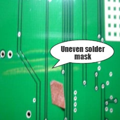
 |
Problem description: Uneven solder mask. Acceptance criteria: 1. When the customer does not have any requirements, the line surface is controlled to be 10um minimum, the line corner is 2.54um minimum, and the substrate is 10um minimum according to internal standards; 2. Green oil is not allowed to accumulate in the component holes and around the patch |
 |
Description of the problem: The circuit is not completely covered by the solder mask, and the bottom copper is exposed. Acceptance criteria: Not allowed, it needs to be repaired with ink, and there should be no obvious color difference after the oil is cured. |
 |
Problem description: There is solder mask on the pad and annular ring. Acceptance criteria: 1. The immersion length of independent square pads on solder mask is 5% or 0.05MM. 2. The surface mount pads on the IC position with a pitch of 21.25MM on the solder mask can only be violated on one side and not more than 0.05MM. 3. The surface mount pads with a pitch <1.25MM can only be violated on one side and not more than 0.025MM. |
 |
Problem description: There is solder mask on the pad and hole ring. Acceptance criteria: 1. The component hole must meet the minimum ring width requirement of 0.05MM; 2. There is no requirement for the via hole. |
 |
Problem description: Solder mask film is reversed. Acceptance criteria: Not accepted. |
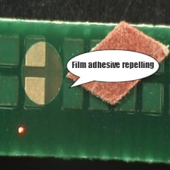 |
Problem description: Solder mask film is reversed. Acceptance criteria: Not accepted. |
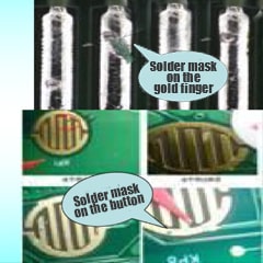 |
Problem Description: There is solder mask on the gold finger, key position, BGA, and MARK point. Acceptance criteria: Not allowed. |
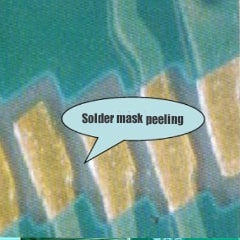 |
Problem description: Solder mask peeling off on the board between SMT trays. Acceptance criteria: 1. For the green oil bridges with a distance between SMT trays <0.635MM, 5 green oil bridges are allowed to be broken for each SMT tray (a group of 4 rows), and 2 consecutive breaks in parallel are not allowed; 2. If the customer has a request, the customer's request will be given priority. |
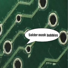 |
Description of the problem: Solder mask wrinkles or very fine bubbles in the solder mask. Acceptance criteria: 1. Tiny bubbles or wrinkles that do not bridge two adjacent wires must be accepted; 2. Use a 3 m tape to test and pull back and forth 3 times without peeling, and the customer has not complained about solder mask bubbles, which is acceptable. |
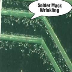 |
Problem description: Solder mask wrinkles or very tiny bubbles in the solder mask. Acceptance criteria: 1. Tiny bubbles or wrinkles that do not bridge two adjacent wires must be accepted; 2. Use a 3 m tape to test and pull back and forth 3 times without peeling, and the customer has not complained about solder mask bubbles, which is acceptable. |
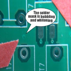 |
Description of the problem: Due to poor adhesion, the solder mask on the circuit is bubbling, whitening or falling off. Acceptance criteria: No falling off when tested with 3M tape. |
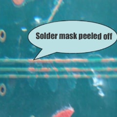 |
Description of the problem: Due to poor solder mask adhesion, the green oil is separated from the copper substrate. Acceptance criteria: No solder mask peeling is allowed in the 3M tape test. |
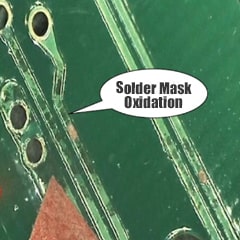 |
Problem description: The circuit on the board under the solder mask shows other colors. Acceptance criteria: Not accepted. |
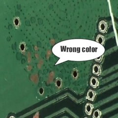 |
Problem description: The circuit on the board under the solder mask shows other colors. Acceptance criteria: Not acceptable. |
 |
Problem description: Debris is sandwiched between the substrate and the solder mask. Acceptance criteria: 1. Debris between two lines does not affect 30% of the line spacing; 2. The maximum size of debris in the solder mask on the board is 0.8MM. |
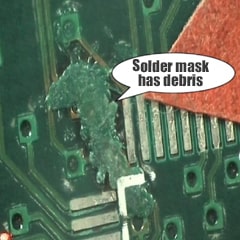 |
Problem description: Debris attached to the surface of the product. Acceptance criteria: 1. Debris between two lines does not affect 30% of the line spacing, and the board is acceptable; 2. The maximum size of debris in the solder mask on the board is 0.8mm. |
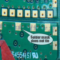 |
Problem description: Solder mask accumulates on the copper surface, causing tin and gold to not be applied. Acceptance criteria: 1. In the case of overall non-solder mask pattern displacement, defects are allowed along 5% of the pads; 2. Defects are not allowed on BGA, SMT pads, gold fingers, key positions, and MARK points. |
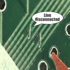 |
Problem description: The line is scratched or disconnected. Acceptance criteria: Not accepted. |
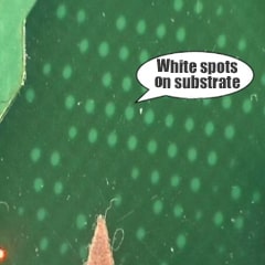 |
Problem description 1. The time in the backwash solution is too long; 2. The backwash temperature is too high; 3. The substrate is dotted. Acceptance criteria: 1. The wire spacing is not lower than the minimum wire spacing value; 2. The distance of microcracks does not exceed 50% of the distance between the conductive patterns of adjacent non-commonly connected circuits; 3. The microcracks on the edge of the board will not reduce the minimum distance between the edge of the board and the conductive pattern; if not specified, it is no more than 2.5MM; 4. The simulated thermal test is not expanded. |
 |
Problem description: Continuous white squares or "+" patterns under the substrate surface. Acceptance criteria: 1. The wire spacing is not lower than the minimum wire spacing value; 2. The distance of microcracks does not exceed 50% of the distance between the conductive patterns of adjacent non-commonly connected circuits; 3. Microcracks on the board edge will not reduce the minimum distance between the board edge and the conductive pattern; if not specified, it is no more than 2.5MM; 4. The simulated thermal test is not expanded. |
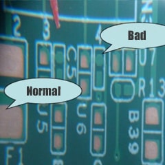 |
Problem description: The pad or text that should be exposed is not exposed. Acceptance criteria: Not accepted. |
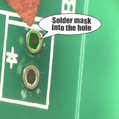 |
Problem description: Solder mask enters the non-plugged hole. (Component hole). Acceptance criteria: 1. Opening windows on both sides: No ink can enter the hole; 2. Opening windows on one side: A small amount of ink can enter the hole, but it must not affect the hole diameter; 3. Opening windows on both sides: It is unacceptable to expose copper on the pad and tin or gold on the pad. |
 |
Problem description: The ink is higher when the via is plugged. Acceptance criteria: BGA, IC position or PAD, button, SMT pad. The ink should not be higher than the pad when plugging the via in BGA, IC, button or SMT, and there should be no bulge when touched. |
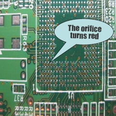 |
Problem description: Light is transmitted through the plugged via, and the hole mouth is red. Acceptance criteria: BGA plugged vias are not allowed to transmit white light, the hole edge is not allowed to be red or the redness ratio of the hole edge is ≤5%. If the customer has special requirements, the customer's requirements shall prevail. |
 |
Description of the problem: There is ink on the film pad. Acceptance criteria: 1. There should be no ink on the test center point; 2. If 95% of the pad area is guaranteed to be welded at the edge of the pad, it is acceptable. |
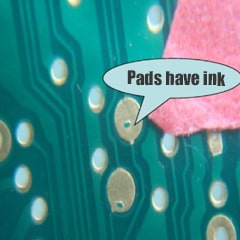 |
Problem description: There is ink on the pad. Acceptance criteria: 1. There should be no ink on the test center point; 2. If the pad edge is guaranteed to have 95% of the soldering surface, it is acceptable. |
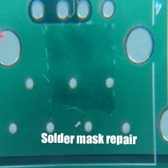 |
Problem description: Solder mask repair is performed due to various surface defects, and the quality after repair does not meet the requirements. Acceptance criteria: Reduce the solder mask repair area to the minimum possible, the maximum repair area is 6.35*6.35MM, 3-5 points on each side, and the thickness cannot be significantly accumulated. |