China 1-40layer PCB/PCBA/EMS/OEM
One stop contract Manufacturing facility
One stop contract Manufacturing facility


+8613798543496


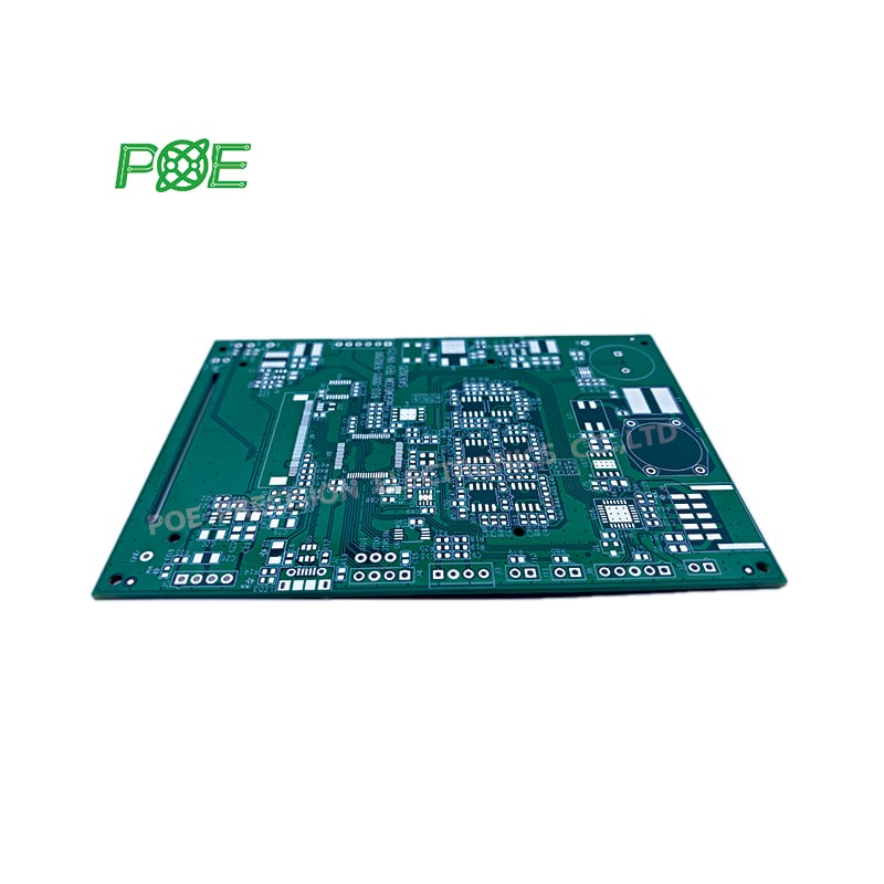
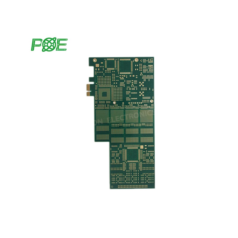
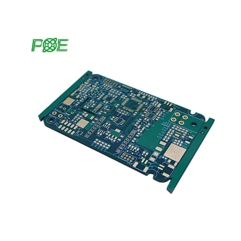
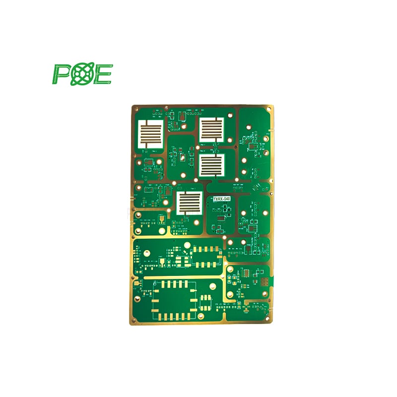
| Layer count | 4 - 40+ layers, with various HDI structures such as 1+N+1, 2+N+2, 3+N+3, and ELIC (Every Layer Interconnect) |
| Base Material | FR-4, High Tg FR-4, Halogen-free, Rogers, or other high-performance materials |
| Board Thickness | 0.2mm - 6.0mm |
| Copper Thickness | 0.5 oz - 6 oz (17.5μm - 210μm) |
| Minimum Hole Size | 0.1mm for mechanically drilled microvias, 0.075mm for laser-drilled microvias |
| Minimum Trace/Space Width | 2 mils (50μm) for standard HDI, down to 1 mil (25μm) for advanced designs |
| Solder Mask | LPI (Liquid Photo-Imageable) in Green, Yellow, White, Black, Blue, Red, and other custom colors |
| Silkscreen | White, Black, Yellow, and other custom colors |
| Surface Finishes | ENIG, OSP, Immersion Silver, Immersion Tin, HASL |
| Blind/Buried Vias | Yes, to enable routing between adjacent or non-adjacent layers |
| Minimum Annular Ring | 2 mils (50μm) for outer layers, 1 mil (25μm) for inner layers |
| Controlled Impedance | Tolerance of ±10% or better |
| Special Features | mbedded or integrated passive components (resistors, capacitors, etc.), rigid-flex designs, back drilling, etc. |

*If you need bare PCB manufacturing + component assembly, then you need to provide gerber file and bom.
Q:Are my PCB Design Files safe when submitting them to you for manufacturing?
A:We respect customer's copyright and will never manufacture PCBs for someone else with your files unless we receive written permission from you, nor we'll share these files with any other 3rd parties.
Q:Do you sign NDA ?
A:Yes.
Q:Do you handle prototype pcbs or Small Volume pcb production orders?
A:Yes, we can manufacture PCBs in any volume.
Q:What kind of file format can you accept?
A:We can process Gerber RS-274X and ODB++ files.
Q:Can you manufacture my board from this: BMP, GIF, TIFF, JPG picture?
A: No, as these formats do not translate to our PCB Fabrication machinery.

Email: all@poe-pcba.com